Semiconductors and the "Depletion Region"
Silicon doesn't conduct well: it's not a conductor like copper (which has lots of free electrons), or an insulator like plastic (which has basically no free electrons), it's a semiconductor. Silicon doped with a few extra electrons ("n-type") conducts current because the electrons move. Silicon doped with a few electron holes ("p-type") conducts current because the holes between electrons move. Silicon without extra electrons or holes is a reasonably good insulator because it's "depleted" of electrons.
If you put p-type silicon next to n-type silicon, and apply a voltage across the two types, something very interesting happens: the electrons and holes can move in opposite directions. With the voltage applied in one direction, both electrons and holes leave the boundary making an insulating "depletion region". If you apply the voltage the other direction, the electrons and holes both converge on the boundary and cancel each other out, conducting current. This is a semiconductor diode! An analogy might be a static front in a war zone, like world war I: as long as soldiers from both sides keep flowing toward the front, they kill each other off and the war continues; if the soldiers of both sides start moving *away* from the front, the front is deserted, and the war's over!
Modern transistors are FET transistors: you charge up a small channel called the "gate", and that electrostatic charge pulls carriers into the depletion region, allowing current to conduct between two terminals (the "source" and "drain"). With the gate uncharged, the depletion region insulates the two terminals, so no current flows.

In an "n-channel FET", you attract electrons to the gate with a positive voltage, to narrow the depletion region and allow it to conduct. In a "p-channel FET", you open the gate with a negative voltage, which pulls holes into the depletion region. I like Logisim or Wikipedia's pictures for these: n-channel is a positive logic input, and p-channel is an inverting input with an inverting circle.
Silicon FET Transistors to Logic Gates
You can build logic gates from FET transistors quite easily in a "totem pole" configuration. Here's an inverter:

When A is positive, it turns off the high gate, disconnecting Q from positive voltage (Vdd); and turns on the low gate, connecting Q to the negative voltage (Vss): A positive makes Q negative. When A is negative, it turns on the high gate and off the low gate, connecting Q to positive voltage and disconnecting negative voltage; A negative makes Q positive.
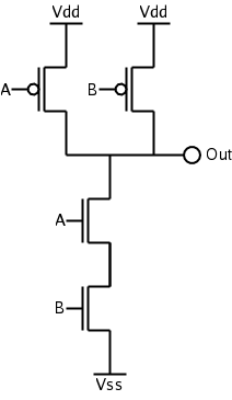
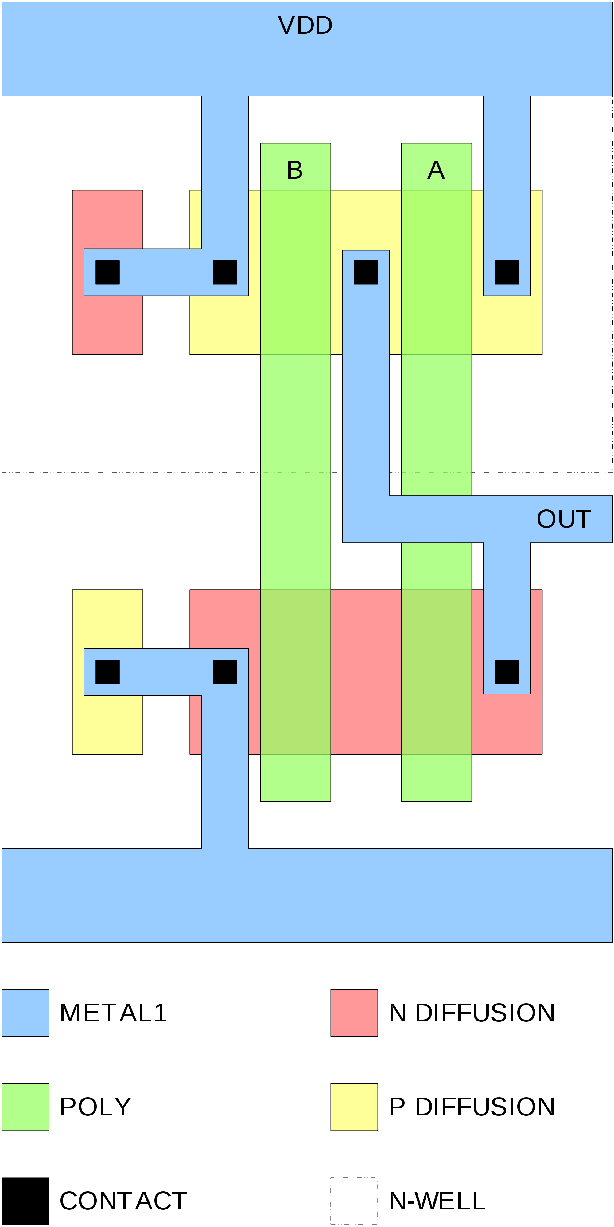
Here's a NAND gate built from FET transistors, and the corresponding silicon implementation:
It's surprisingly easy to build all the logic gates with FET transistors!
Until 2017, I showed an AND gate on this page, but on real chips designers tend to use NAND gates instead of AND gates. They do this because like an inverter, NAND happens to need the active-low PMOS transistors on the high side, and the active-high NMOS transistors on the low side--this makes the transistor gate voltages large, which rapidly and efficiently switches the transistor completely on (called saturation mode). By contrast, if you try to put an active-high NMOS transistor on the high side, all the pins of the transistor are high, so the transistor doesn't really turn on. This has a bad enough impact on the gate's analog characteristics that when real chip designers need to build an AND gate, they just use a NAND followed by an inverter!
Why do you care? Speed!
In a real circuit, the FETs all have some capacitance at the gate, and all the wires in the circuit have some resistance. This means it takes a certain amount of time for the transistor to switch. This Falstad circuit simulator CMOS inverter shows this behavior with fairly plausible values, resulting in overshoot and slow switching rise times. Note the switching speed drops as the core voltage drops; but the switching speed improves as the gate capacitance drops (e.g., as the transistors get smaller).
Latchup
There's an annoying phenomenon called "latchup" where the current going through a logic gate output can leak back to the input and keep the gate open. The affected circuit is then stuck in this state until you turn the power off.
I encountered a latchup error in the memory subsystem of my GPU one summer: the machine had been running fine for weeks, when suddenly it started giving bad output from programs. Initially, of course, you suspect the program is at fault, but going back to a known-good version it still failed. A memory tester program revealed tons of memory errors, so I suspected the graphics card driver (a new beta version) had corrupted itself, so I rebooted the machine. This was a warm boot, the only kind you can perform over the network (remember that it's summertime, so I'm not in my office). It didn't fix the problem--the memory errors were still there just like before the reboot. At this point, I realized: it's not software, it's hardware! The next trip into my office, I powered the machine off, waited a few seconds (to clear the latchup), and the powered it back on. Problem solved.
In April 2010 a similar bug may have affected Galaxy 15, a satellite in geosynchronous orbit that stopped responding to commands. Over a period of months, it drifted off course while still broadcasting at full blast. Eventually, the satellite lost orientation control, so the solar panels no longer faced the sun, drained its own batteries, and rebooted itself in late December. It now seems fine, possibly the victim of a cosmic ray induced latchup (a known hazard for space computers).
Modern Silicon
Traditionally, every 2 years, manufacturers have doubled the number of transistors they can fit onto the same area of silicon.
Several companies are currently shipping "10nm" semiconductors. Nothing on a "10nm" semiconductor is actually 10nm in size, but it is tiny. 10nm was "late", arriving more than 2 years after the previous node of 14nm due to a variety of problems with the tiny size. 7nm is the next node, but it's widely considered the last node for silicon.
In 2015 they officially published the last (!) International Technology Roadmap for Semiconductors; previously they'd publish a new report every 2 years, but now it's not clear what to do next. One atom is about 0.1nm in size, so single-atom variations are already causing problems with semiconductors.
Modern semiconductor design is starting to require extensive feedback up and down the design layers.