Intel Core i7
In November 2008, Intel released their most recent family of processors, the Core i7 line, codenamed Nehalem. With the i7 came several innovations in the field of consumer processors.
The most significant difference brought with the i7 is the elimination of the north bridge or memory controller hub (MCH). To accomplish this, Intel developed onboard memory and PCI-e controllers. Basically, the purpose of a memory controller is to perform DRAM refreshing as well as reading and writing to memory, while the PCI-e controller interfaces with the GPU. Without exception, going all the way back in Intel’s history, the memory and graphics controllers have been left up to the motherboard manufacturer to implement. With this change, memory and graphics latency have been both reduced and standardized, with the only cost being that the current i7 family is only compatible with DDR3 memory. Below are two diagrams, the left being the older architecture type, and the right being the newer i7.
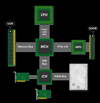
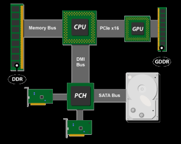
This evolution was groundbreaking not just for Intel but for the entire processing market; though other manufacturers had implemented the memory controller onboard in the past, none had included the graphics controller onboard as well. With this change it seems the next step would be to integrate even more components onto the processor die, which Intel plans to do with their next processor line by including a GPU onboard the CPU die starting with the Arrandale family.
Another significant difference between i7 and the previous models is the number of cores on the die. Where both the Core and Core 2 series offered single and dual core setups, with the latter offering quad core only on their high-end models, i7 was introduced with four cores on all the difference performance levels. What this means is that there isn’t such a vast difference in performance between the different versions of the i7, including those destined for mobile devices, which is a good thing for the consumer. This was intended by Intel, as in the past it’s been difficult for those who aren’t totally computer savvy to understand what they are getting. This was particularly the case with the E, L, P, Q, T, U, and X series of the Core 2s as can be seen here.
The next big difference implemented in the i7 line is the Shared L3 Cache. In previous Intel quad-core implementations, the processor cores would each get their own L1 cache (which is still the case), then split off into pairs to share two L2 caches, but it ended there. This was sufficient as long as the paired cores only passed data to one another, but if cores 1 or 2 needed to pass data to cores 3 or 4, the bits had to be sent out to the front side bus and then back to the other pair. With the i7, a third cache was implemented which is shared between all of the cores. With CPU intensive multi-core code, this new cache can allow fairly significant performance increases. Below is an actual die diagram of the new i7.
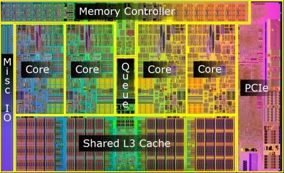
Here one can see all of the components covered thus far, with the four cores in the middle. Overall, the mainstream i7 processor boasts a whopping 731 million transistors, up from 291 million in the Core 2 Duo. All this new hardware may lead one to wonder how they fit it all onto the same processor die, and the answer is, really they didn’t. With both the later Core 2 and the early i7 architectures using the same 45nm manufacturing technology, the only way to fit all the new components onto one die was to make the die physically larger.
The changes made with the i7 don’t just stop there though. In early 2003, Intel introduced a method of dual-core emulation with just one processor core for their Pentium 4 series, which they called Hyper-threading. This provided a significant performance increase with minimal added cost (15-20% speed for 5% die area) and was a smashing success. With the introduction of multi-core processors, this technology was abandoned because there actually were two cores, and it was deemed unnecessary. With the higher end i7 processors, Hyper-threading is back. Though the performance increase isn’t quite as phenomenal, the difference from emulating eight cores for parallel CPU intensive tasks is non-trivial. There are also more budget-friendly models that exclude Hyper-threading, but they are clearly separated from the i7 and fall under the i5 nomenclature.
Other improvements include the reduction in the number of pipeline stages, down to fourteen from the “bloated” peak of thirty-one in the last models of the Pentium 4. This reduced the cost of branch prediction misses by almost half, and increased the number of operations done per processor cycle by the same amount. With the clock rate race from the Pentium 4 era over, this is the direction Intel has gone to stay competitive in the market, and for the past four years, this direction has kept Intel firmly in the lead of the consumer market.
Notable links:
http://www.bit-tech.net/hardware/cpus/2009/09/08/intel-core-i5-and-i7-lynnfield-cpu-review/1
http://en.wikipedia.org/wiki/Intel_Core_i7
http://en.wikipedia.org/wiki/Intel_Nehalem_%28microarchitecture%29
http://en.wikipedia.org/wiki/Hyper-threading
http://en.wikipedia.org/wiki/List_of_Intel_Core_2_microprocessors
http://en.wikipedia.org/wiki/Transistor_count
http://www.tomshardware.com/reviews/intel-core-i5,2410.html