The idea of the Cell was originally coined by Sony as a next generation processor for the PlayStation 3. In addition to gaming, Sony also wanted a processor that could suit all sorts of applications. Similarily, Toshiba wanted to cut costs by manufacturing the processor for all their electronic devices themselves. Sony, Toshiba, and IBM cooperated to develop the Cell.
Both Sony and Toshiba produce many different kinds of electric appliances, and wanted to cut production costs by being able to produce a single processor that could work with any electric device. Sony and Toshiba had lots of experience manufacturing and marketing, while IBM had lots of experience in chip design.
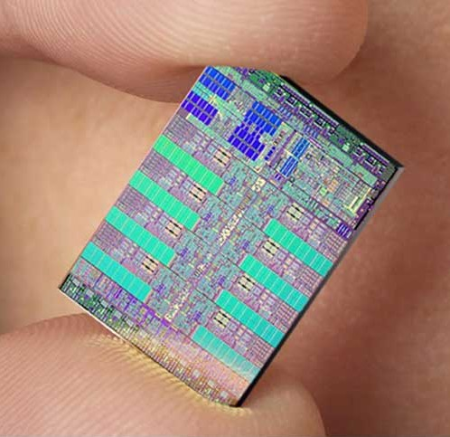
The first technical disclosures of the Cell were released in 2005.About $400 million has already been invested in the design and development since 2001 [1] .
The Cell architecture was designed with an emphasis on providing power efficient and fast data processing for a low production cost.
While the Cell initially gained its fame in the PlayStation 3, the Cell is also used in many other applications.
Some of the types of computations that IBM claims the Cell is specialized for are as follows,Some of the fields that IBM claims the Cell is applicable: [3]
IBM boasts that the Cell is several magnitudes faster than current processor architectures running the same applications. The PowerXCell 8i processor can taain 205 GFlops per second per processor running at single precision and 100 GFLops per second running at double precision. IBM claims that the Synergistic Processor elements are about an order of magnitude faster than other processors that use SIMD instructions [3]
One of the key objectives in the development of the Cell processor was to overcome the memory wall that was limiting performance. Fast CPUs such as the IBM POWER or Intel Itanium waste about 80% of their time waiting for something to come from memory [8]. Thus, no matter how fast you make the CPU, memory will always be the limiting factor.
The Cell is geared towards fast performance of single precision floating point computations.
Furthermore, the Cell boasts clock speeds of over 4 ghz. The Cell inside of the Playstation 3 is clocked at 3.2 ghz. The Cell consumes around 60-80 watts at 4 ghz with one PPE and 7 SPEs [8] .
One of the reasons for the lower power consumption when compared to other processors is the simpler architecture. In Intel and AMD processors, an immense amount of circuitry is used to determine which instructions are indepndent of each other and thus can be executed simultaneously. The Cell processor does not do such analysis of instructions. Rather, the Cell primarily relies on the compiler to provide 'hints' to the Cell in order to maximize efficiency [8] .
 [4]
[4]
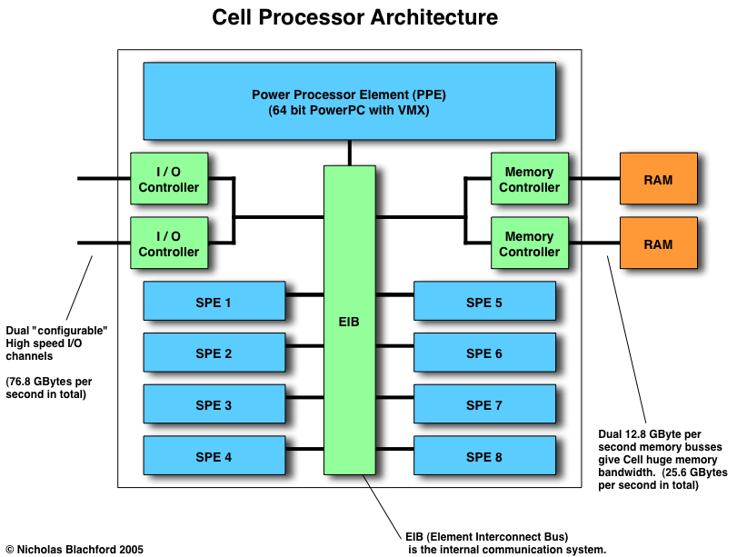
SIMD (Single Instruction, Multiple Data, AKA, 'vector instructions') are parsed and fed into the SPEs from the PPE.
Interestingly, the Cell does not use any sort of memory cache. Rather, DMA commands go between main memory and private local memory to the processor that is used to store both instructions and data. The SPE instruction fetching and load-and-store instructions access private local memory rather than shared main memory.
Once of the radical changes in processor architecture that is present in the Cell that the workhorse processors contain their own private local memory that is asynchronous with main memory. Thus, the workhorse processors instruction-fetches and load & store instructions access their own private memory rather than main memory. Thus, computation of data and transfer of data is effectively paralleled.
With computation being done in local memory, and data being asynchronously transferred between between local memory and main memory, the huge latency factor associated with main memory is no longer a problem [3] .
According to IBM, "The most productive processor memory-access model is one in which a list of DMA transfers is constructed in the processor's local store, so that the processor's DMA controller can process the list asynchronously while the processor operates on previous transferred data." [3]
 [1]
[1]
[2] IBM Cell Installation Guide -
[3] Cell Broadband Engine Solution
[5] IBM Research – The Cell Architecture