Simple CPU Design
CS 641 Lecture, Dr. Lawlor
Circuit Simulation via TkGate
We're really not going to do spend much time designing actual digital
circuits (this isn't an EE course!), but it's important to understand
the general way digital logic circuits work.
The easiest way to do this is to just play around with circuits for a
few hours. I've prepared the examples below using TkGate, a UNIX-ey
open source digital logic designer and simulator.
- In Windows, TkGate is only available via the UNIX compatability layer Cygwin, but it is built in to Cygwin.
- In Linux, TkGate is often available from your package manager (in Ubuntu, "sudo apt-get install tkgate").
- In MacOS X, supposedly TkGate can be built from source, which you download here.
The TkGate Documentation is pretty good, and the program runs a simple tutorial when you start it.
Many other circuit simulators exist. In EE 341, I used "LogicWorks",
which is a fine commercial program for Windows and MacOS. Sadly, translating
circuits between two graphical simulator packages is only rarely possible!
Simple CPUs built from Digital Logic Circuits
Here are a few steps on the evolutionary path to a CPU:
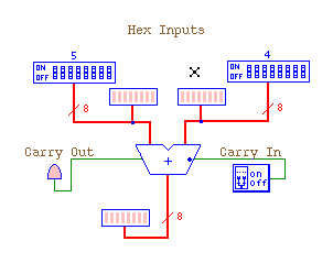
First, an add circuit. We've set up two 8-bit hex input devices
(DIP Switches) in TkGate, hooked them to a Make -> ALU -> Adder,
and displayed both input and output binary data in 8-LED arrays.
Click the above circuit to download the TkGate Verilog-style circuit
description.
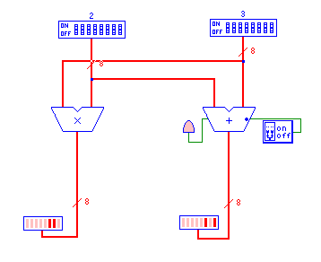
Here's almost the same circuit, except now we run the input values past a multiply circuit as well as the adder.
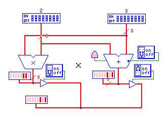
Now we've added a "bus". The little three-input triangles below each arithmetic unit are "tri-state buffer/drivers",
which enable us to turn the add and multiply outputs on and off, and so
combine the outputs of these two circuits. The idea is we turn on
the output we want, which at the moment we do manually, by flipping the
appropriate output switch. If you turn multiple outputs on at the
same time, or turn no outputs on, TkGate shows a yellow indeterminate
output state. In real circuits, driving a bus to several
different values causes the buffer drivers to heat up and possibly fry
themselves!
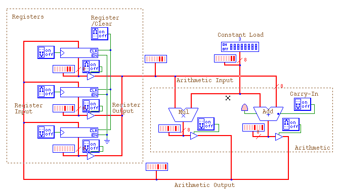
Now we add a set of "registers", which are just data storage
elements. We hook up the output of each register to a tri-state
driver, and use the drivers to select which register we want to read as
input. We hook up the data input to each register to the
arithmetic output bus. Finally, we can manually "clock in" the
arithmetic result into any register (via the triangle-shaped register
inputs).
Annoyingly, TkGate starts all the registers in indeterminate (yellow)
state, rather than zero, so we have to manually clear the registers at
simulated startup by flipping the register clear switch off and then on
again.
OK, now we're approaching a real CPU! The only thing we're
missing is a control unit that will flip all the switches appropriately
to execute some instructions!
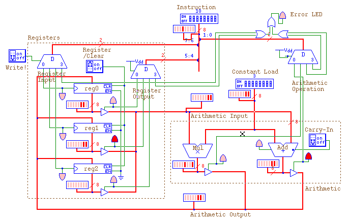
The big trapezoidal "0 D 3" modules are called decoders
(also known as demultiplexors or demuxes). They take a binary
input value (the red bus going in the top), and copy the left input to
one of the four outputs along the bottom. We've wired these mux
outputs to the input lines of our arithmetic bus, register output bus,
and register input bus. This means that rather than manually
flipping switches, we just need to load a binary number into the
"instruction" register!
In this case, we've connected bits 1:0 (the low two bits) of the
instruction to the arithmetic operation demux. So if the low bits
are 00, the add circuit turns on. If the low bits are 01, the
multiply circuit turns on. Bits 5:4 (the low two bits of the high
hex digit) connect to the register output. So 00 means output
register 0 to the arithmetic input bus, 01 means output register 1, 10
means output register 2, and 11 is an error. Finally, bits 7:6,
the high two bits of the instruction, connect to the register input
control lines. To write to register 0, the high bits should be
zero, and so on. You need to manually flip the "write" switch to
make the registers write (this avoids annoying circuit race conditions).
So overall, this CPU's instructions look like:
<destination register: 2 bits>
<source register: 2 bits> <unused: 2 bits>
<operation: 2 bits>
<constant: 8 bits>
For example, the instruction (hex) "40" (binary 0100 0000) writes to register 1, reads from register 0, and adds.
CPU Design Philosophy
A CPU is actually a very simple circuit that continually does exactly two things:
- Figure out what to do next. (fetch)
- Do it. (decode and execute)
CPU's usually encode "what to do next" in a chunk of binary data called a machine language instruction, almost always stored in memory somewhere. CPUs usually have a special register, the "program counter" or "instruction pointer", that points to the address in memory with the instruction to execute next.
So "Figure out what to do next" just means "Load the next instruction
from the memory address at the instruction pointer." The
instruction pointer is usually moved to point to the next instruction
as part of this "fetch" phase.
"Do it" just means to decode the machine language instruction and figure out what it's telling you to do, then actually do what it says (execute). We've basically got that under control in the TkGate circuit above.
A Trivially Simple CPU Emulator: UEMU
A full-fledged CPU emulator can be written in just a few dozen lines of
C++. For example, here's the core of "UEMU", a silly little
made-up CPU I wrote a few years ago:
int CPU::run(void) {
while (1) {
int inst=mem[regs[0xf]++]; /* instruction fetch */
int opcode=(inst>>12)&0xf, i=(inst>>8)&0xf,
j=(inst>> 4)&0xf, k=(inst>>0)&0xf;
switch (opcode) { /* instruction decode */
case 0x1: regs[i]=(inst&0xff); break; /* "load Immediate" */
case 0xA: regs[i]=regs[j]+regs[k]; break; /* Addition */
case 0xC: if (regs[j]>=regs[k]) regs[i]++; break; /* Cond */
case 0xE: /* Emulator (or OS) call: */
switch (i) {
case 0x0: printf("%d%c",regs[k]," \n\t,"[j]); break;
case 0x1: printf("Enter a value:\n");
scanf("%i",®s[k]); break;
case 0xD: dump(inst&0xff); break;
case 0xE: return regs[k]; /* Emulator Exit */
default: quit("Unknown OS-trap instruction 0x%X at 0x%X!\n",inst,regs[0xf]-1);
};
break;
default: quit("Unknown instruction 0x%X at 0x%X!\n",inst,regs[0xf]-1);
};
}
}
(Try this in NetRun now!) or just download the source code and run it yourself.
"regs" is a little array of registers. "mem" is another little array of memory locations.
If you look at the decode step, it should eventually become clear that
executing an instruction like "0x1234" will be an "Immediate" load
instruction (case 0x1:), loading into register 0x2 the value 0x34.
Similarly, "0xA234" will Add into register 2 the contents of registers 3 and 4.
Memory
Used only for storing program instructions. UEMU is a bit odd in
that memory consists of 16-bit instructions, not 8-bit bytes.
Normally a single instruction (or integer) stored in memory spans
several bytes, but not in UEMU!
Registers
There are 16 registers numbered 0 through F (in hex). Register F
is the program counter--it stores the memory address of the next
instruction to execute. Note that loading a new value into
register F will cause a jump! All other registers are free for
programmer use.
Instructions
The instruction encoding is chosen such that everything's a multiple of
4 bits long, which makes it easy to write machine language programs in
hex. There are a ridiculously small number of instructions:
- 0x1ikk: IMMEDIATE. Assign the "immediate" 8-bit value kk to register i. For example,
0x1307 would assign the value 0x07 to register 3. Note that
0x1Fkk assigns to the program counter, and is hence a jump instruction.
- 0xAijk: ADD. Add registers j and k, and assign the result to register i. For example,
if registers 2 and 3 hold values 0x40 and 0x50, 0xA123 puts the sum
0x90 into register 1. Note that 0xA111 doubles the value of
register 1.
- 0xCijk: CONDITIONAL INCREMENT. If register j is greater
than or equal to register k, increment register i. For example,
if register 2 is 0x40 and register 3 is 0x50, 0xC232 increments
register 2 to 0x40, while 0xC223 does nothing. Note that
incrementing the program counter (0xCFjk) conditionally skips the next program instruction.
- 0xE0jk: EMULATOR OUTPUT. Print the value in register k in
decimal, followed by a space if j==0, a newline if j==1, a tab if j==2,
and a comma if j==3. For example, 0xE012 prints the value of register 2 in decimal followed by a newline.
- 0xE10k:
EMULATOR INPUT. Read a value from standard input into register
k. Accepts decimal, hex, and octal using the C convention.
For example, 0xE105 loads a value into register 5.
- 0xEDkk: EMULATOR DUMP. Dump out the values of all the
registers. If kk==0, dumps out the program memory as well.
If kk=0xFF, does nothing.
- 0xEE0k: EMULATOR EXIT. Stop running the emulator, but print out the value in register k.
A tiny software emulator like this is a good way to get the feel for how to design a CPU instruction set.